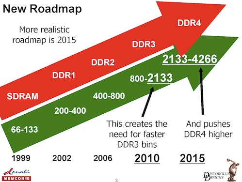
Based on the first chart, it appears that the consensus of manufacturers expect DDR4 to really hit the market in 2015. In other words, none of these IC specifications should be anything for system builders to be concerned over for quite some time.
The JEDEC standards group has announced its intentions to finalize the DDR4 specification sometime in 2011 and begin commercial production in 2012. However, the next generation DDR4 SDRAM memory technology is expected to introduce a radical change to the topology of the chipset memory subsystems on desktops, notebooks and in enterprise server environments. As bit-tech mentioned back in April, Intel's upcoming Sandy Bridge-E platform based on socket LGA 2011 is expected to feature quad-channel DDR3 memory, or one DIMM per channel in order to maximize memory bandwidth available to the rest of the system. This type of implementation would require a Point-to-Point memory controller design, where parallelism shifts from the DIMM channels to the memory controller itself.

Source: bit-tech
In order to compensate for high memory capacity in the enterprise server marketplace, it is expected that server motherboards will use high performance digital switches to distribute memory controller processing to a larger number of channel nodes. The concept is very similar to the PCI-Express switches that have been implemented over the years, and many will probably recall Nvidia's NForce 200 chip performing a nearly identical function for distributing more lanes to high-bandwidth GPUs. However, analysts are expecting the server implementation to use some form of error checking and correction due to the complexity of the subsystem topology.

Source: PC Watch
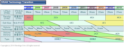
As far as performance is concerned, we can expect DDR4 memory to scale up to and possibly over 4.266GHz speeds by 2015. While JEDEC continues its work on finalizing the performance aspect of the next-generation standard, it is expected that DDR3 should receive a new frequency standard that should scale all the way up to 2133MHz at just 1.25v. By this time, DDR4 will have just been introduced to the market (the enthusiast market, we should say) and will continue the performance roadmap around DDR4-2133MHz at 1.20v. As PC Watch notes, however, there is a misconception between how much voltage is decreasing in the technology roadmap versus how much power consumption is increasing relative to the original PC-133 at 3.3v memory specification. Although DDR4 2133MHz memory at 1.20v seems like a significant accomplishment for JEDEC and industry giants, the standard actually consumes four times more power for performance than SDR 133MHz memory did at 3.3v so long ago. In essence, it is the quality of the size reductions on future advanced processing nodes at 28nm and below that will determine the scale of efficiency for future memory modules.

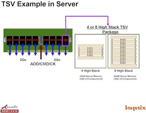
In addition to the high-bandwidth performance gains we can expect from the transition to DDR4 in a few years, the new standard features a 3D chip stacking technique that should allow much higher GB capacities than ever before. Introduced by Intel in late 2006, Through-hole Silicon Via (TSV) is a low-cost, highly economical vertical electrical connection technology used to stack large quantities of CPU cores and memory ICs on top of one another in 3D space. In a nutshell, it allows memory manufacturers to stack ICs in vertical pillers so they occupy less space. As a result, the market's adoption of the technology could lead to a day where single 64GB memory modules are available to enterprise server environments, allowing memory capacity to scale up way beyond its current chipset limits.

Source: PC Watch
All in all, there are still several design concerns that DRAM manufacturers need to address when scaling down to more advanced process nodes. With the introduction of TSV stacking, IC leakage poses a greater threat to DRAM stability than it does in its current state. It would also produce more heat in relation to package density, and we expect heatsinks will need to be redesigned with extensive research affordances in order to compensate. Analysts have also predicted that 3D IC stacking can lead to lower overclocks and lower voltage walls for enthusiast system builders. All of these questions remain to be determined over the next few years, and as semiconductor manufacturers continue to progress towards denser IC packages, stability concerns in relation to Moore's Law will become the forefront of design success.


