Thursday, August 3, 2006
What is Fully Buffer DIMM?
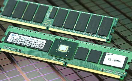
FB-DIMMs represent the next-generation server memory technology that is currently being standardized by JEDEC, the industry's standard group. Intel is a key developer of FB-DIMM technology and the first adopter, launching it on its two-way Xeon servers (code-named "Bensley") with 5000 series chipsets launching in 2006. FB-DIMMs are "intelligent" memory modules, incorporating a special memory controller built into the memory module.
The Fully Buffered DIMM (FB-DIMM) interface is a high speed (2.4 to 4.8GT/s) narrow (67)pin interface. This enable double the number of memory channels on a given chipset. For example, the first FB-DIMM chipset has 4 memory channels in place of two on DDR2 chipsets.
FB-DIMMs are not compatible with existing servers utilizing DDR2 Registered DIMM memory. They also will not work in desktop or mobile platforms as they are only designed for servers with FB-DIMM memory architecture.
Memory Channel Architecture
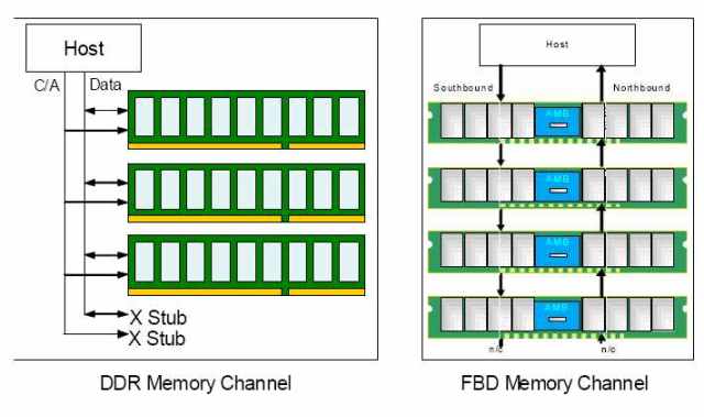
Traditional memory solutions are based on stub bus architecture with up to 4 DIMMs per memory channel. The maximum frequency of a 4 DIMM channel is around 266Mhz (clock). At higher frequencies channel capacity degrades to 3, 2 and eventually one DIMM per channel. FB-DIMM overcomes this limitation by moving to a high speed serial interface. Each DIMM has a buffer (Advanced Memory Buffer or ‘AMB’) that decodes/encodes data for local DRAMs and re-drives high-speed data to the next DIMM in the chain. That means a nominal motherboard can have 8 DIMM slots instead of 4 DIMM slots. For server application, this is extremely important.
The serial interface consist of several channels of input signal call the “North bound lanes” and output signal call the “South bound lanes”. They are of extremely high frequency in the Giga Hertz range. Once the high-speed signal reaches the Advanced Memory Buffer IC (on board of the DIMM), the signal is converted back to the conventional parallel memory bus. This parallel memory-bus only have to drive one set of memory chips in a simple “point to point” manner.
This architecture does not only apply to modules using DDR2 memory, but would also apply to the future DDR3 memory. For distinction, the DDR2 FB-DIMM is called FB-DIMM 1. The AMB that goes with it is called the AMB1. While for the DDR3 generation, they will be called FB-DIMM 2 and AMB2.
Test Challenges
The extremely high speed at the serial interface makes the module very difficult to test by conventional method or conventional memory tester. Since the memory chips are hidden behind the AMB, it makes it difficult to detect any short and opens plus actual memory cell failures. At the same time, since DRAMs are now mostly in BGA package, operator no longer can pinpoint the bad solder joint by visual inspection. The only conclusion, in this case, would be to built-in Design For Test (DFT) mechanism. Fortunately, the DFT functions can be implemented into the AMB chip and can be executed through it.
AMB designers have come up with the following basic DFT strategies:
- FB-DIMM must be testable using conventional equipment and methods.
- DFT will allow testing over traditional methods with traditional testers at both component and at DIMM level.
- Memory BIST (Built In Self Test) to be used during buffer, DIMM test and system test.
- Transparent mode, which allows access to the DRAM behind the buffer.
- IBIST (Built In Self Test for Interconnect Bus) used for interconnect testing at DIMM and system level.
- LAI (Logic Analyzer Interface) mode allows the AMB to act as an intelligent front end for logic analyzer.
FB-DIMM Test Using a CTC Board (Channel Test Card)
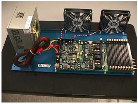
Intel designs a Channel Test Card (CTC) for triggering the DFT functions on the AMB. It is available through a 3rd party manufacturer. The CTC is mainly used to activate the functions on the AMB. It provides the necessary power supply voltages to the DIMM. It sets up the AMB self test functions through the SMBus . It also controls which DIMM slot is to be tested.
FB-DIMM IO Test
Once setup, the AMB’s IBIST signal generator generates a high-speed signal into the interconnect bus. The signal is looped back and verified. Thus the high-speed transmission lanes can be proven. These are all done with supplying a reference clock signal of 100Mhz to 200Mhz from the CTC.
DDR Interface Test
Memory access can be tested with the MBIST (Memory Built-In Self Test) function built into the AMB. Through the CTC, a reference clock signal is supplied to the AMB. At the same time, the CTC can setup a certain memory test patterns to be written into the memory cells at the output of the AMB. The CTC can also command a read back to examine the simple test patterns at full speed. Due to the very high speed execution, only limited number of complex patterns can be generated by the MBIST. This test is therefore, not recommended for full DRAM array testing.
DRAM Array Test
There are tests to be performed to confirm the connection between the AMB and the DRAMs. They are done in the “Transparent Mode”. The AMB is designed with a switch to reroute some of the high-speed channels into slower speed pass-through mode. This is called the “transparent mode”. In this mode, a DC leakage test can be performed to verify fundamental assembly errors like shorts and opens between the AMB output and the DRAMs.
Through the transparent mode, the DRAM array and each cell can be tested through a reduced speed testing. This mode allows a test speed of 200Mhz clock and 400Mhz data rate. The data and test pattern is generated by an external (standard) memory tester at 16 bit wide. The transmission can also be multiplexed to achieve a full 64bit data word together with ECC. The read back is through an accumulator built-in to the AMB. The AMB checks the read back data against the written data and sets a flag for any error. Therefore, the external testers load is greatly reduced. Complex test patterns can also be used to cycle out the memory array errors at the memory core.
Programming the SPD
The FB-DIMM would not function properly in a system until the SPD (serial presence detect) bytes are programmed properly. A comprehensive understanding of FB-DIMM SPD bytes is important. SPD specifications are available from your memory manufacturer and from JEDEC standard. SPD programmers are usually built-in with most memory module testers. They are almost identical to the previous generation SPD programmers with the difference in the SPD byte table.
Motherboard Validation
Since there is no full speed test performed along the FB-DIMM test flow, motherboard validation test is a must. Motherboard test will exercise the module in real environment including extreme speed and heat generation. 4-corners voltage condition test is good to ensure the modules will operate at various power supply tolerance. Interoperability test is also required as modules made with AMB from different sources can also generate problem. This test is done by plugging modules with different vendor AMB into different slots on the motherboard.
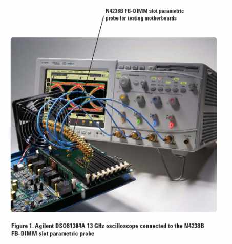
Oscilloscope and Logic Analyzer Monitoring
Memory engineers might like to directly probe the signal paths for signal integrity, timing and waveform. This is done with fixture supplied by Agilent. Agilent supplies a special FBDIMM probe card to intercept the signals for measurement without disturbing the FB-DIMM functions. The probe card is built with module gold pin interface on one side, and high-speed signal connection to instruments on the other side. It also utilizes the LAI (Logic Analyzer Interface) mode at the AMB to trigger the oscilloscope or the logic analyzer.
Conclusion:
Due to the very high speed, there is no “one test for all” on FB-DIMM. Instead, it should be first tested through the CTC tester. It then has to go through a transparent mode tester for functional array test and leakage measurement. The final step is SPD programming and system board validations. Only and only then the FB-DIMM can be qualified for ultimate functionality.
For more information on thr FB-DIMM Specifications click on this Intel Website
http://www.intel.com/technology/memory/FBDIMM/spec/Intel_FBD_Spec_Addendum_rev_p9.pdf
By: DocMemory
Copyright © 2023 CST, Inc. All Rights Reserved
|