Friday, August 25, 2006
Introduction
Since I wrote “Understanding DDR Serial Presence Detect (SPD) Table” in 2003, I have been getting a lot a feedback from readers. Some of you told me that you are using this article to train your employees,
and to introduce the mysteries SPD concept to your customers. I feel honored by your responses.
Lately, some of you had encouraged me to add the DDR2 SPD Table. Since the DDR2 DIMM has taken mainstream recently, I think this is the time to add an article for the DDR2 SPD Table. Due to the many more years of development, the DDR2 SPD table has definitely got more sophisticated than the original DDR SPD table. Your attention is required to understand and follow through. I will try to use as much layman language, as I can to accommodate you all.
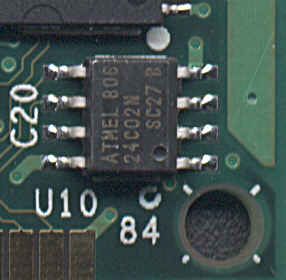
Picture of a 8pin-SPD EEPROM made by Atmel
Serial Presence Detect (SPD) data is probably the most misunderstood subject in the memory module industry.
Most people only know it as the little Eprom device on the DIMM that often kept the module from working properly in the computer. On the contrary, it is quite the opposite. The SPD data actually provide vital information to the
system Bios to keep the system working in optimal condition with the memory DIMM. This article attempts to guide you through the construction of an SPD table with “Turbo-Tax” type of multiple choices questions. I hope you’ll find it interesting and useful.
Byte 0
Number of Serial PD Bytes written during module production
This field describes the total number of bytes used by the module manufacturer for the SPD data and any (optional)
specific supplier information. The byte count includes the fields for all required and optional data.
For most manufacturers, they do not insert optional data and the resulting data (in hex) would normally be:
128Byte: 80h 256Byte: FFh
Byte 1
Total number of Bytes in Serial PD device
This field describes the total size of the serial memory used to hold the Serial Presence Detect data,
device used is usually 128 Bytes or 256 Bytes with 256 Bytes as the most common.
256 Byte (24C02)
(34C02) with Software Write Protect function
(34C02B)with Reversible Software Write Protect function : 08h
128 Byte (24C01): 07h
Byte 2
Fundamental Memory Type
This refers to the DRAM type. In this case, we are only dealing with DDR2 SDRAM.
DDR2 SDRAM: 08h
Byte 3
Number of Row Addresses on this assembly
This relates to the DRAM size as well as the Refresh scheme of the DRAM.
The best way to discover this is to use the AutoID function of the CST DIMM tester.
You would first run the AutoID on the tester.
You then use the [Edit] [AdrDat] function to display the Row and Column Address counts.
15: 0Fh 14: 0Eh 13: 0Dh 12: 0Ch
Byte 4
Number of Column Addresses on this assembly
This relates to the DRAM size as well as the Refresh scheme of the DRAM.
The best way to discover this is to use the AutoID function of the CST DIMM tester.
You would first run the AutoID on the tester. You then use the [Edit] [AdrDat] function
to display the Row and Column Address counts. 13: 0Dh 12: 0Ch 11: 0Bh 10: 0Ah 09: 09h
Byte 5
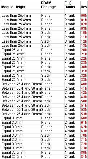
Module Attributes - Number of Physical Banks on DIMM, Package and Height
This is a multi-purpose field that involves calculations and bit combination.
A Flash program combine them together and give you an automatic result after
you have selected the different attributes.
Byte 6
Module Data Width of this assembly
This refers to the number of data bit width on the module. For a standard 8 byte DIMM, 64 bits
would be most common while an 8 byte ECC module would have 72 bits. Some special module might
even have up to 144 bits. In any case, a CST tester Auto ID function would tell you this number
in plain English.
32 bit: 20h 64 bit: 40h 72 bit: 48h 144 bit: 90h
Byte 7
Reserved
Not available: 00h
Byte 8
Voltage Interface Level of this assembly
This refers to the power supply voltage Vdd of the DIMM. Standard DDR2 SDRAM module would be SSTL 1.8V
1.8V DDR2: 05h Recommended Default
Byte 9
SDRAM Device Cycle time
This commonly referred to the clock frequency of the DIMM. Running at its specified CL latency.
5.0 ns (400Mhz): 50h 3.75 ns (533Mhz): 3Dh 3.0 ns (667Mhz): 30h
2.5 ns (800Mhz): 25h
Byte 10
SDRAM Device Access from Clock (tAC)
This byte defines the maximum clock to data out time for the SDRAM module. You can normally
read off the tAC specification on the Timing Parameter table.
+/-0.6 ns: 60h
+/-0.5 ns: 50h
+/-0.45 ns: 45h
+/-0.40 ns: 40h
Byte 11
DIMM Configuration Type
This is to identify the DIMM as ECC, Parity, or Non-parity. Normally non-parity is related to
64 bit module, Parity and ECC are related to 72 bit or higher memory bit width on the module.
NonECC: 00h
ECC: 02h
Address/Command Parity with ECC: 06h
Byte 12
Refresh Rate
This byte describes the module's refresh rate and if it is self-refreshing or non-self refreshing.
Today, most standard modules would be capable of self-refreshing. The refresh time is easily read
from the DRAM manufacturer data sheet. Refresh time can be listed in two different ways.
1. In Refresh Interval Time. For example: 15.6usec. or 7.8usec.
2. In milli-seconds per x Refresh Cycles. For example: 62.4ms in 8K refresh
This can be converted back into refresh interval time with the equation:
Refresh Interval = Total Refresh Period/number of refresh cycles.
15.6 us Self-refresh (4K): 80h 7.8 us Self-refresh (8K): 82h
15.6 us non Self-refresh : 00h 7.8 us non Self-refresh : 02h
Byte 13
Primary SDRAM Width
This refers to the bit width of the primary data SDRAM.
For a standard DIMM module. 4 bits: 04h 8 bits: 08h 16 bits: 10h
Byte 14
Error Checking SDRAM Width
This refers to the bit width of the error checking DRAM. For a standard module,
it is either no ECC bit, or 8 bits on a regular 8 byte module. It can also be 16 bits on
a 144 bit (16 byte) module.
No-ECC: 00h 8bits: 08h 16bits: 10h
Byte 15
Reserved
Not available: 00h
Byte 16
Burst Lengths Supported
This is indicates the burst length supported. In DDR2, standard DRAM are all 4, 8 burst supported.
4, 8 Burst length supported: 0Ch
Byte 17
Number of Banks on SDRAM Device
This is referring to the internal bank on the DRAM chip. All modern DDR2 chips under 1Gbit have
4 internal banks. For chips at 1Gbit or above, they have 8 internal banks.
4 Internal Banks: 04h 8 Internal Banks (for 1Gb or 2Gb chips only): 08h
Byte 18
CAS Latency (CL)
This refers to the all the different Cas Latency supported by your chip. This can vary with the
frequency you operate your DIMM. This number can be read off your DRAM data sheet.
CL=3 and 4 supported: 18h
CL=4 and 5 supported: 30h
CL=5 and 6 supported: 60h
CL=5 supported: 20h
CL=6 supported: 40h
Byte 19
DIMM Mechanical Characteristics
This defines the module thickness where the maximum thickness includes all assembly parts: devices,
heat spreaders, or other mechanical components. This information together with the DIMM type, allows
the system to adjust for thermal operation specifications.

Byte 20
DIMM type information
This byte identifies the DDR2 SDRAM memory module type.
Each module type specified in this Byte 20 defines a unique index for module thickness specified in Byte 19,
which may be used in conjunction with thermal specifications in Bytes 21 and 47-61 to adjust system operation
conditions based on installed modules.
Undefined 00h
Regular Registered DIMM: 01h
Regular Unbuffered DIMM: 02h
SO-DIMM: 04h
Micro-DIMM: 08h
Mini-Registered DIMM: 10h
Mini-Unbuffered DIMM: 20h
Byte 21
SDRAM Module Attributes
This byte involves 4 main items. Bit 0-1 signifies the number of registers on the DIMM. Bit 2-3 signifies
the number of PLL’s on the DIMM. Bit 4 indicates if any on board FET switch is enabled. Bit 6 indicates
if an analysis probe is installed. In most cases, Bit 4 and Bit 6 are not used.
The resulting hex code is calculated as follows:
0 PLL chip and 1 Register chip 00h
0 PLL chip and 2 Register chip 01h
1 PLL chip and 1 Register chip 04h
1 PLL chip and 2 Register chip 05h
2 PLL chip and 1 Register chip 08h
2 PLL chip and 2 Register chip 09h
Byte 22
SDRAM Device Attributes –General
This byte is a multi-purpose byte. It includes PASR (Partial Array Self Refresh) , 50 ohm ODT enable and
also support of Weak Driver. The resultant hex code is calculated based on the selection you made.
Supports PASR Supports 50 ohm Supports weak driver HEX
No No No 00h
No No Yes 01h
No Yes No 02h
No Yes Yes 03h
Yes No No 04h
Yes No Yes 05h
Yes Yes No 06h
Yes Yes Yes 07h
Byte 23
SDRAM Min Clock Cycle at CLX-1
This is referred to the speed (or frequency) the DRAM can run at when the Cas Latency
is reduced by 1 clock. This data can be looked up from the datasheet of the DRAM.
This is usually listed at the first page of the data sheet where it mentioned highest
frequency it can run at a certain Cas latency setting.
De-rated latency
3.0ns (667 Mhz): 30h
3.75 ns (533Mhz) : 3Dh
5.0 ns (400Mhz) 50h
Undefined: 00h
Byte 24
Max Data Access Time(tAC) at CLX-1
This is referred to DQ output access time from CK/CK* at when the Cas Latency is reduced by 1 clock.
This data can be looked up from the datasheet of the DRAM. This is usually listed as tAC on the data
sheet where it mention maximum frequency it can run at a certain CAS latency setting.
+/-0.45ns: 45h +/-0.5 ns: 50h +/-0.6 ns: 60h Undefined: 00h
Byte 25
SDRAM Min Clock Cycle at CLX-2
This is referred to the speed the DRAM can run at when the Cas Latency is forced to reduce by two notches.
This data can be looked up from the datasheet of the DRAM. This is usually listed at the first page of the
data sheet where it mentioned the frequency it can run at a certain Cas latency setting.
3.75 ns (533Mhz): 3Dh 5.0 ns (400Mhz): 50h Undefined: 00h
Byte 26
Max Data Access Time(tAC)CLX-2
This is referred to DQ output access time from CK/CK* at when the Cas Latency is reduced by 2 clock.
This data can be looked up from the datasheet of the DRAM. This is usually listed as tAC on the data
sheet where it mention maximum frequency it can run at a certain CAS latency setting.
+/-0.45ns: 45h +/-0.5 ns: 50h +/-0.6 ns: 60h
Byte 27
Minimum Row Pre-charge Time (tRP)
This is tRP min read off the DRAM data sheet.
15 ns: 3Ch
Byte 28
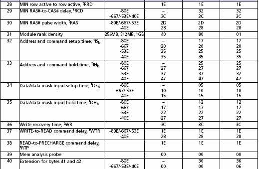
Minimum Row to Row Access Delay (tRRD)
This is the tRRD min time read off the DRAM data sheet.
(x4,x8) 7.5ns: lEh (x16) 10 ns: 28h
Byte 29
Minimum Ras to Cas Delay (tRCD)
This is the tRCD min time read off the DRAM data sheet
15 ns: 3Ch
Byte 30
Minimum Active to Pre-charge Time (tRAS)
This is the tRAS min time read of the DRAM data sheet.
40 ns: 28h (For DDR2 533/400Mhz)
39 ns 27h (For DDR2 667 Mhz)
Byte 31
Module Bank Density
This refers to the Mega-Byte in each physical bank (per rank) on the DIMM.
For example: if a 256MB module has two physical banks, then each physical bank
should have 128MB.
128MB: 20h 256MB: 40h 512MB: 80h
1G: 01h 2G: 02h 4G: 04h
Byte 32
Address and Command Input Setup Time Before Clock (tIS)
This refers to the time of the address and command lines have to occur before the
next clock edge. It is labeled as tIS min in the case of DDR2.
DDR2 (tIS) 0.2ns: 20h 0.25 ns: 25h 0.30 ns: 30h 0.35 ns: 35h
Byte 33
Address and Command Input Hold Time After Clock (tIH)
This refers to the period of time the address and command lines have to hold after
the last clock edge has appeared. It is labeled as tIH min in the case of DDR2.
0.275 ns: 27h 0.325ns: 32h 0.375 ns: 37h 0.475 ns: 47h
Byte 34
SDRAM Device Data/Data Mask Input setup Time Before Data Strobe (tDS)
This refers to the time of the Data and Data Mask lines have to occur before the
next clock edge. It is labeled as tDS min in the case of DDR2.
DDR2(tDS) 0.05ns: 05h 0.10 ns: 10h 0.15 ns: 15h
Byte 35
Address and Command Input Hold Time After Clock (tDH)
This refers to the period of time the Data and Data Mask lines have to hold after
the last clock edge has appeared. It is labeled as tDH min in the case of DDR2.
DDR2(tDH)0.175ns: 17h 0.225 ns: 22h 0.275 ns: 27h
Byte 36
Write recovery time (tWR)
This byte describes the write recovery time(tWR)min
15.0 ns: 3Ch
Byte 37
Internal write to read command delay (tWTR)
This byte describes the internal write to read command delay (tWTR)min
7.5 ns: 1Eh 10.0 ns: 28h
Byte 38
Internal read to pre-charge command delay (tRTP)
This byte describes internal read to precharge command delay
(tRTP) 7.5 ns: 1Eh
Byte 39
Memory Analysis Probe Characteristics
This byte describes various functional and parametric characteristics of the memory
analysis probe connected to this DIMM slot. These characteristics may be consulted
by the BIOS to determine proper bus drive strength to account for additional bus
loading of the probe. It also describes functional characteristics of the probe that
may be used to configure the memory controller to drive proper diagnostic signals to
the probe, such as via the TEST,NC pin
Not available: 00h Default value if probe is not described
Byte 40
Extension of Byte 41 tRC and Byte 42 tRFC
This byte serves as an extension when Byte 41 or Byte 42 has run out of space to
accommodate the bigger value
When tRFC (byte 42) is 127.5ns, byte 40 is: 06h
When tRFC (byte 42) is 327.5ns, byte 40 is: 07h
When tRC (byte 41) is 63.75ns, byte 40 is: 50h
When tRC (byte 41) is 65ns, byte 40 is: 00h
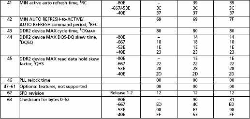
Byte 41
Minimum Active to Active Auto Refresh Time (tRCmin)
53ns: 35h 54ns: 36h 55 ns: 37h 60 ns: 3Ch
63.75ns: 8Eh 65ns: 41h
Byte 42
Minimum Auto Refresh to Active Auto Refresh Time (tRFC)
This byte identifies the minimum Auto-Refresh to Active/Auto-Refresh Command Period (tRFC).
(256Mb)75 ns: 4Bh (512Mb)105 ns: 69h
(1Gb) 127.5ns: 7Fh (2Gb) 195ns: C3h
(4Gb) 327.5ns: 47h
Byte 43
Maximum Device Cycle time (tCKmax)
8 ns: 80h
Byte 44
Maximum Skew Between DQS and DQ (tDQSQ)
Maximum DQS tolerance.
0.24 ns: 18h 0.30 ns: 1Eh 0.35 ns: 23h
Byte 45
Maximum Read DataHold Skew Factor (tQHS)
Maximum DOS and DO window tolerance.
0.34 ns: 22h 0.40 ns: 28h 0.45 ns: 2Dh
Byte 46
PLL Relock Time
This refers to the lock time on the PLL IC used in the registered module.
You can read this off the PLL device datasheet.
Undefined: 00h 8us: 08h 10us: 0Ah
12us: 0Ch 15 us: 0Fh
Byte 47 to Byte 61
These bytes describe the thermal characteristic of the memory chips and the logic
chips used on the module. These are complex thermal data used in calculating the
thermal throttling of the microprocessor speed under overstress conditions. In most systems,
these data are ignored (or not available).
Byte 47
Tcasemax
Bits 7:4: Tcasemax Delta, the baseline maximum case temperature is 85 OC. Bits 3:0: DT4R4W Delta.
Not available: 00h
Byte 48
Psi T-A DRAM
Thermal resistance of DRAM device package from top (case) to ambient (Psi T-A DRAM)
Not available: 00h
Byte 49
DTO/Tcase Mode Bits
Bits 7:2:Case temperature rises from ambient due to IDDO/activate-pre- charge operation minus 2.8 OC
offset temperature. Bit 1: Double Refresh mode bit. BitO High Temperature self-refresh rate support
indication
Not available: 00h
Byte 50
DT2N/DT2Q
Case temperature rises from ambient due to IDD2N/precharge standby operation for UDIMM and due to
IDD20/precharge quiet standby operation for RDIMM.
Not available: 00h
Byte 51
DT2P
Case temperature rises from ambient due to IDD2N/precharge standby operation for UDIMM and due to
IDD20/precharge quiet standby operation for RDIMM.
Not available: 00h
Byte 52
DT3N
Case temperature rises from ambient due to IDD2P/precharge power-down operation
Not available: 00h
Byte 53
DT3Pfas
Case temperature rises from ambient due to IDD3P Fast PDN Exit/active power-down with Fast PDN
Exit operation
Not available: 00h
Byte 54
DT3Pslow
Case temperature rises from ambient due to IDD3P Slow PDN Exit/active power-down with Slow PDN
Exit operation
Not available: 00h
Byte 55
DT4R/Mode Bit
Bits 7:1: Case temperature rises from ambient due to IDD4R/page open burst read operation.
Bit 0: Mode bit to specify if DT4W is greater or less than DT4R
Not available: 00h
Byte 56
DT56
Bits 7:1: Case temperature rises from ambient due to IDD4R/page open burst read operation.
Bit 0: Mode bit to specify if DT4W is greater or less than DT4R
Not available: 00h
Byte 57
DT7
Case temperature rise from ambient due to IDD7/bank interleave read mode operation
Not available: 00h
Byte 58
Psi T-A PLL
Thermal resistance of PLL device package from top (case) to ambient (Psi T-A PLL)
Not available: 00h
Byte 59
Psi T-A Register
Thermal resistance of register device package from top (case) to ambient (Psi T-A Register)
Mot available: 00h
Byte 60
DT PLL Active
Case temperature rises from ambient due to PLLin active mode atVCC = 1.9 V the PLL loading is the DIMM loading
Not available: 00h
Byte 61
DT Register Active/Mode Bit
Bits 7:1: Case temperature rises from ambient due to register in active mode at VCC = 1.9 V,
the register loading is the RDIMM loading. Bit 0: mode bit to specify register data output toggle rate 50% or 100%
Not available: 00h
Byte 62
SPD Data Revision Code
Revision 1.0: 10h Revision 1.1: 11 h Revision 1.2: 12h
Byte 63
Checksum for Byte 0 to 62
Checksum is calculated and placed into this byte. All CST testers have automatic checksum calculation for this byte.
All you have to do is to fill in and audit byte 0-62, the tester will automatically fill in byte 63 for you
through the auto-checksum calculation.
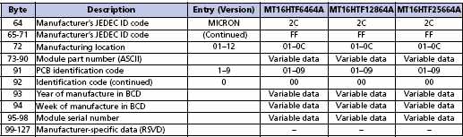
Byte 64-71
Manufacturer’s JEDEC ID Code
This is a code obtained through manufacturer’s registration with JEDEC ( the standard setting committee).
A small fee is charged by JEDEC to support and maintain this record. Please contact JEDEC office.
Byte 64 is the most significant byte. If the ID is not larger then one byte (in hex), byte 65-71 should be
filled with 00h.
Byte 72
Module manufacturing Location
Optional manufacturer assigned code.
Byte 73-90
Module Part Number
Optional manufacturer assigned part number.
The manufacturer’s part number is written in ASCII format within these bytes. Byte 73 is the most
significant digit in ASCII while byte 90 is the least significant digit in ASCII. Unused digits are
coded as ASCII blanks (20h).
Byte 91-92
Module Revision Code
Optional manufacturer assigned code.
Byte 93-94
Module Manufacturing Date
Byte 93 is the year: 2005 69h 2006 6Ah 2007 6Bh
Byte 94 is the week of the year: wk1-wk15 01h – 0Fh
wk16-wk31 10h – 1Fh
wk32-wk47 20h – 2Fh
wk48-wk52 30h – 34h
Byte 95-98
Module Serial Number
Optional manufacturer assigned number.
On the serial number setting, JEDEC has no specification on the data format nor dictates
the location of Most Significant Bit. Therefore, it’s up to individual manufacturer to
assign his numbering system. All CST testers and EZ-SPD programmers have the option for
user to select either byte 95 or byte 98 as the MSB (most significant bit). The testers
assume the use of ASCII format; which is the most commonly used. The CST testers also have
the function to automatically increment the serial number on each module tested.
Byte 99-127
Manufacturer’s Specific Data
Optional manufacturer assigned data.
Byte 128-255
Open for Customer Use
Optional for any information codes.
Final Note:
Everything in the above article and more are now implemented into the CST EZ-SPD DDR2
Programmer software. The new features are:
1. Pop up window of explanation on each Byte.
2. Clickable selection right from the illustration window.
3. Auto checksum on byte 62.
4. Text input on "manufacturer code" and "serial number". User define MSB/LSB format.
5. Auto JEDEC week and year coding from PC clock.
6. Software write protect function.
.....just to name a few.
For further information, please view : www.simmtester.com
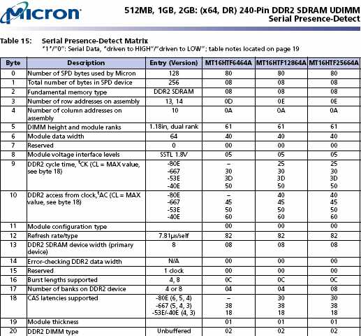
DDR2 SPD table reference from Micron Technology
Byte 21- 27

Byte 28 -40
Byte 41 - 63
Byte 64- 127
By: DocMemory
Copyright © 2023 CST, Inc. All Rights Reserved
|