Following DDR and DDR2 memory, the next synonym on PC memory is, of course, “DDR3”. While Intel has promised delivery of DDR3 memory system on PC’s in Q207, the picture is still not clear. This article examines the difference between DDR2, DDR3, and performance difference on using DDR3. It also predicts the consumer sentiment and adaptation time table.
Difference between DDR2 and DDR3
Higher operational frequency
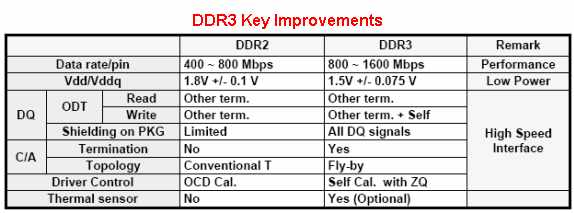
According to JEDEC, DDR3 will be running at 800MHz to 1666 MHz. That would double the frequency of DDR2. This will bring operational performance to systems by slashing the read and write time into half.
Lower voltage and power
DDR3 operates at 1.5V instead of the 1.8V for DDR2. The power saving factor is, therefore, 16%. This will offset the higher power consumption brought by increasing the operational frequency. At the same time, die shrinking will also help in power reduction to give DDR3 twice the performance per watt of power.
DDR3 is also built-in with power conservation features like partial refresh. Precious system battery power will no longer need to spend on refreshing the portion of the DRAM not in active use. It also included a thermal sensor to allow the system to provide minimum refresh cycles when the system is not in high performance demand thus to achieve further power saving.
More internal banks
To further speed up the system, DDR3 consist of 8 internal banks vs 4 internal banks on DDR2. As the size of the DRAM increases, this will allow advance pre-fetch to reduce access latency.
Mode register difference
Because of the many feature selections, the initialization on DDR3 takes a new approach. The Mode Registers (MRS) are re-engineered for quicker and more efficient configuration of the memory system.
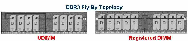
Modules on fly-by topology
For the higher frequency operations, DDR3 is now more critical on signal integrity of the memory module (DIMM). At the extreme frequencies, the signal path can no longer be balanced, but have to be tuned (trained) to match to each DRAM. The module signal path topology is called the “fly-by” vs. “T branches” as on the DDR2 module. That means the address and control lines will be a single path chaining from one DRAM to another instead of the T topology that branches on DDR2 modules. This method takes away the mechanical line balancing and turn to automatic signal time delay generated by the controller fixed at the memory system training. Each DDR3 DRAM has an automatic leveling circuit for calibration and to memorize the calibration data.
Technical difficulties on DDR3 memory systems
To achieve maximum memory efficiency on the system level, system front side bus frequency has to follow suit. The most optimum is to have the front side bus run at the memory data execution frequency. That is 800MHz to 1600MHz. That puts the burden on the processor and also the chipset. On the other hand, higher frequencies also mean more signal integrity issues. Both motherboard and module design engineers now have to deal with strip line, micro strip, termination impedance and return loss….all those new radio frequency terms. Test equipment for verification of the circuit is no longer available at low costs. Engineer often require $100,000 of equipment just to look at the memory performance.
The “Fly-By” timing technology puts the burden on system calibration. Memory system is calibrated each time the computer is turned-on. The controller and the DRAM circuit design allow the calibration to be done in an automatic mode. To make this calibration, extra circuit and intelligence has to be added to the controller and to the DRAM. Extra die area on the chip is also required to accommodate. This might add cost to the final system.
As the speed of the DRAM memory system increases, so as the amount of Cache memory built onto the MPU. New processors come with 1MB to 2MB of on-board cache memories. That means there might be no main memory hit during normal non-graphical operations. Therefore, one might never see the performance increase with faster DRAM at normal applications. The memory technology might have reached a point of diminishing return.
Another point of system argument is number of memory slots required for the system. DDR3 specification calls for maximum of 2 two rank modules per channel at the lower frequency of 800MHz to 1333MHz. Only one memory slot is allowed at the maximum operational frequency of 1600MHz.
The Address/Command on DDR3 unbuffered modules are in a “single fly-by path” while DDR3 registered modules are routed in a T split before getting to the individual DRAM. Therefore, the registered system is more complicated. The registered chips now also have to be trained to compensate for the individual DRAM timing. The registered module is not only built with the clock buffer (PLL) on the same die but also have configuration registers to set the training parameters.
In summary, there will be technical frontiers to be tested during the initial implementation of DDR3 memory technology.
DDR3 adoption driven by application
Overall, DDR3 mass adoption should be driven by applications and pricing. The power reduced feature is best suited for Notebook and Mobile multi-media applications. As handset and mobile devices gets multi-media heavy, DDR3 will find its place. Price is also another factor. Consumer market reception of new technology is often related to price. As DDR3 becomes main stream, a derivative of it will be used for graphic applications found in future handset and set-top boxes.
Since the early DDR3 frequencies (800MHz and 1066MHz) will overlap with DDR2, consumer will not find much interest in rushing to the same performance. Mass adoption will only come at 1333MHz and higher.
DDR3 price performance curve
According to price/performance, DDR3 sweet spot is seen at 2Gbit chips. For DRAM vendors to produce 2Gb chips at acceptable power consumption level, 50nm to 60nm semiconductor line width will have to be used. This will become a schedule and investment challenge to the DRAM producer. At this point, it is forecasted that the smaller geometry would not be cost effective until late 2008. That will essentially mean DDR3 would not cross price parity with DDR2 nor in mass adoption before Q4/08.
DDR3 as mainstream memory
DDR3 as mainstream will be delayed. Industry will likely extend the life of DDR2 for PC applications. Breakthrough will probably come when DDR3 lands on consumer mobile application like Mobile IPTV, portable streaming receiver, or portable game devices.